Scientists have shown that twisting a crystal at the nanoscale can turn it into a tiny, reversible diode, hinting at a new era of shape-engineered electronics.
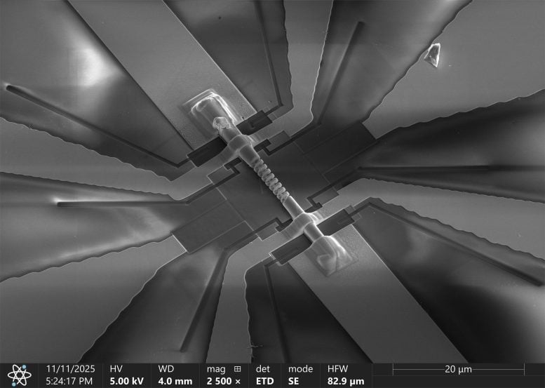
Researchers at the RIKEN Center for Emergent Matter Science, working with collaborators, have created a new technique for building three-dimensional nanoscale devices directly from single crystals. The approach uses a focused ion beam instrument to precisely carve materials at extremely small scales.
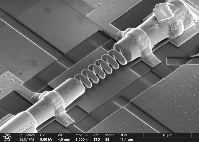
Using this method, the team shaped tiny helical structures from a topological magnetic material made of cobalt, tin, and sulfur, known by its chemical formula Co₃Sn₂S₂. Tests revealed that these structures behave like switchable diodes, allowing electric current to pass more easily in one direction than the other.
Why Three-Dimensional Nanostructures Matter
Building electronics with complex three-dimensional shapes could lead to devices that are smaller, faster, and more energy efficient. Until now, however, only a limited number of fabrication techniques could create such structures. Many of those methods restrict which materials can be used and often reduce the quality of the final device, limiting their practical impact.
A Nanoscale Sculpting Tool
In the new study, published in Nature Nanotechnology, the scientists turned to a focused ion beam capable of cutting with sub-micron accuracy. This allowed them to overcome many of the existing limitations. In principle, the technique makes it possible to shape three-dimensional devices from almost any crystalline material. The process works much like traditional sculpture, with the ion beam carefully removing material until the desired form emerges.
Helical Shapes Create Switchable Diodes
To show what the method could do, the researchers fabricated helical nanodevices from the magnetic crystal Co₃Sn₂S₂. Based on the material’s properties, they expected the twisted shape to produce an unusual diode effect known as nonreciprocal electrical transport, which arises from the chiral geometry at the nanoscale.
Their experiments confirmed this idea. Electric current flowed more easily in one direction than the other, and the effect could be reversed by changing either the magnetization or the handedness of the helix. The team also observed the opposite interaction, where strong electrical pulses were able to flip the magnetization of the structure. Diodes play a central role in modern electronics, including AC/DC conversion, signal processing, and LED technology.
How Shape Influences Electron Motion
By studying helices of different sizes and testing them across a range of temperatures, the scientists linked the diode behavior to uneven electron scattering along the curved walls of the devices. The results show that the physical shape of a component can directly influence how electricity moves through it. This insight suggests new ways to design low power electronic elements by engineering geometry itself, with potential applications in future memory, logic, and sensing systems.
Geometry as a New Design Principle
According to Max Birch, the study’s first author, “By treating geometry as a source of symmetry breaking on equal footing with intrinsic material properties, we can engineer electrical nonreciprocity at the device level. Our newly developed focused ion beam nanosculpting method opens up a wide range of studies on how three-dimensional and curved device geometries can be used to realize new electronic functions.”
Research group leader Yoshinori Tokura added, “More broadly, this approach enables device designs that combine topological or strongly correlated electronic states with engineered curvature in the ballistic or hydrodynamic transport regime. The convergence of materials physics and nanofabrication points to functional device architectures with potential impact on memory, logic, and sensing technologies.”
Reference: “Nanosculpted 3D helices of a magnetic Weyl semimetal with switchable non-reciprocal electron transport” 21 January 2026, Nature Nanotechnology.
DOI: 10.1038/s41565-025-02104-x
Never miss a breakthrough: Join the SciTechDaily newsletter.
Follow us on Google and Google News.