Researchers developed a new fabrication technique to overcome design and performance challenges for scalable single-photon detectors.
New fabrication techniques for arced-fractal SNSPDs are improving <span class="glossaryLink" aria-describedby="tt" data-cmtooltip="
” data-gt-translate-attributes=”[{"attribute":"data-cmtooltip", "format":"html"}]” tabindex=”0″ role=”link”>photon detection, boosting <span class="glossaryLink" aria-describedby="tt" data-cmtooltip="
” data-gt-translate-attributes=”[{"attribute":"data-cmtooltip", "format":"html"}]” tabindex=”0″ role=”link”>quantum computing and secure communications. Scientists have optimized materials and processes, making these detectors more efficient than ever.
Revolutionizing Electronics with Photon Detection
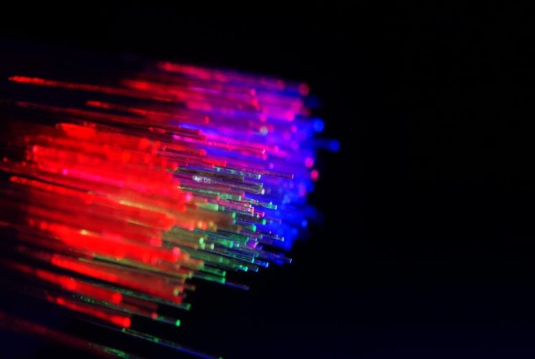
Light detection plays a crucial role in modern technology, from high-speed communication to quantum computing and sensing. At the heart of these systems are photon detectors, which identify and measure individual light particles (photons). One highly effective type is the superconducting nanowire single-photon detector (SNSPD). These detectors use ultra-thin superconducting wires that instantly switch from a superconducting state to a resistive state when struck by a photon, enabling extremely fast detection.
To enhance performance, the nanowires in these detectors are arranged in a Peano arced-fractal pattern, a unique structure that remains consistent across different scales. This fractal design allows SNSPDs to detect photons regardless of their direction or polarization (the orientation of their electric field), making them highly versatile. Because of their superior speed and sensitivity, arced-fractal SNSPDs (AF SNSPDs) are widely used in technologies like quantum computing, secure communication, and light detection and ranging (LiDAR).
A recent study, published in the IEEE Journal of Selected Topics in Quantum Electronics, offers a detailed guide to fabricating high-quality AF SNSPDs. Conducted by Professor Xiaolong Hu and Dr. Kai Zou from Tianjin University, China, the research outlines the materials, fabrication techniques, and key challenges involved in building these advanced detectors.
“This paper aims to present the nano- and micro-fabrication developments of high-performance fractal SNSPDs, with particular emphasis on the important experimental details that are key to the success of these devices,” says Prof. Hu.
Inside the Structure of AF SNSPDs
AF SNSPDs consist of three components: nanowires for photon detection, optical microcavities to capture photons, and keyhole-shaped chips that house and align the detector with the optical fiber. The fabrication process begins with creating the optical microcavity by coating a silicon wafer with six or eight alternating layers of silicon dioxide (SiO2
The nanowires are patterned into a fractal design using scanning-electron-beam lithography and then transferred to the NbTiN layer through reactive-ion etching. The microcavity is completed by depositing a top SiO2 defect layer and additional alternating layers of Ta2O5/SiO2 using aligned optical lithography and IBD. The chip is shaped into its keyhole form using optical lithography, inductively coupled <span class="glossaryLink" aria-describedby="tt" data-cmtooltip="
” data-gt-translate-attributes=”[{"attribute":"data-cmtooltip", "format":"html"}]” tabindex=”0″ role=”link”>plasma etching, and the Bosch etching process, and packaged for optical fiber connections.
Optimizing Performance for Maximum Efficiency
The authors also provided suggestions for optimizing the fabrication processes of nanowires, optical microcavities, and keyhole-shaped chips. Some of their recommendations include: Applying a 5-nm silicon or 3-nm SiO2 layer as an adhesion promoter to improve bonding between the resist patterned into nanowires and the NbTiN material, using auxiliary AF nanowire patterns to ensure consistent nanowire widths, and a careful design of the layout and spacing for optical microcavities to minimize photoresist deformation. They also suggested using accurate alignment markers for keyhole-shaped chips and gradually applying heat during the curing process to enhance photoresist stability and minimize etching defects.
A Bright Future for Quantum Technology
In conclusion, the researchers were able to develop SNSPDs with impressive sensitivity and system detection efficiency. “These advancements will help simplify the fabrication of fractal SNSPDs enabling the development of more advanced devices with additional functionalities,” says Prof. Hu.
Such steady improvements in SNSPD design and fabrication can pave the way to breakthroughs in quantum computing, telecommunications, and optical sensing. The future of photonics sure looks bright!
Reference: “Fabrication Development of High-Performance Fractal Superconducting Nanowire Single-Photon Detectors” by Kai Zou and Xiaolong Hu, 25 December 2024, IEEE Journal of Selected Topics in Quantum Electronics.
DOI: 10.1109/JSTQE.2024.3522176