
The introduction of a nanometric germanium oxide layer drastically improved device performance and stability.
As the global demand for clean energy accelerates, solar power continues to attract attention because it is widely available and can be scaled to meet growing needs. Alongside this push, scientists have increasingly explored thin-film solar cells as an alternative to conventional crystalline silicon devices. These thinner designs can be produced at lower cost, show more consistent manufacturing outcomes, and are well-suited for use in lightweight and flexible electronic applications.
Among the candidate materials, tin monosulfide (SnS) has emerged as a strong option for next-generation thin-film solar cells. It is inexpensive and non-toxic, setting it apart from more established technologies that depend on limited elements such as indium, gallium, and tellurium. SnS-based devices also align with the United Nation’s Sustainable Development Goals and, based on their fundamental properties, should be capable of efficiently absorbing sunlight.
In practice, however, SnS solar cells have not yet delivered the performance levels predicted by theory. Experimental results have consistently lagged behind expectations, despite years of research and optimization. One of the primary obstacles is found at the rear-contact interface, where the SnS layer meets the metal electrode.
At this critical junction, several issues arise simultaneously. Structural imperfections, undesirable chemical reactions, and the uncontrolled movement of atoms all interfere with the smooth flow of electrical charges. Together, these problems reduce how effectively the device can collect and transport energy, placing a significant limit on overall solar cell efficiency.
A New Interface Engineering Strategy
Against this backdrop, a research team led by Professor Jaeyeong Heo and Dr. Rahul Kumar Yadav from Chonnam National University, Republic of Korea, has made a substantial breakthrough in thin-film solar cell design. Their study, published online in Small, describes an innovative approach, which centers on inserting an ultra-thin layer of germanium oxide (GeOx) between the molybdenum back contact and the SnS absorber layer.
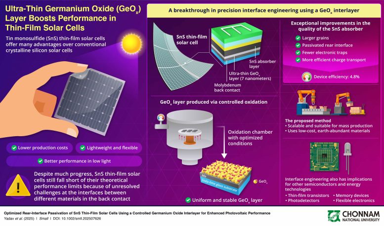
The researchers employed a precise yet simple method to create this 7-nanometer thick GeOx interlayer. They exploited the natural oxidation behavior of a thin Ge film in a vapor transport deposition process, which is scalable and industry-friendly.
“Despite its nanoscale thickness, this interlayer addresses several long-standing challenges at once,” explains Prof. Heo. “It suppresses harmful deep-level defects, blocks unwanted sodium diffusion, and prevents the formation of resistive molybdenum disulfide phases during high-temperature fabrication.”
These combined effects dramatically improve the quality of the SnS absorber, leading to larger, more uniform grains, enhanced charge transport and collection, and a significant reduction in electrical losses.
Efficiency Gains and Broader Implications
The implementation of this controlled GeOx interlayer resulted in a substantial boost in power conversion efficiency, increasing from 3.71% in standard devices to an impressive 4.81%. This marks one of the highest efficiencies reported for SnS-based solar cells produced using vapor deposition methods.
Notably, the ability to engineer precise material interfaces has wide-ranging implications beyond solar cells. For example, metal/semiconductor interfaces in thin-film transistors determine contact resistance and switching performance. Similarly, favorable interfacial properties are essential for high energy conversion efficiency in thermoelectric devices, sensitivity and charge transfer in sensors, mechanical stability in flexible electronics, and performance in photodetectors and memory devices.
“Across all these applications, mastering the metal/semiconductor interface remains central to advancing next-generation devices,” says Prof. Heo. “We believe that this work will open new avenues for research, contributing to the development of advanced solar cells and other key technologies.”
Reference: “Optimized Rear-Interface Passivation of SnS Thin-Film Solar Cells Using a Controlled Germanium Oxide Interlayer for Enhanced Photovoltaic Performance” by Rahul K. Yadav, Vishesh Manjunath, Yong Tae Kim, Girish U. Kamble, Wookyung Jeon, Parag R. Patil, Neha Bisht, Jin Hyeok Kim, Yohan Yoon and Jaeyeong Heo, 19 September 2025, Small.
DOI: 10.1002/smll.202507626
Never miss a breakthrough: Join the SciTechDaily newsletter.
Follow us on Google and Google News.