
New optical chip enables ultra-fast computing and data processing. Built using silicon photonics for next-gen networks.
The rise of the big data era presents major challenges for information processing, particularly in terms of handling large volumes of data and managing energy consumption. These issues are further compounded by the fact that over 90% of data is transmitted using light waves, while the actual processing still predominantly occurs in the electrical domain. To address this mismatch, two main approaches have emerged. One involves converting signals from optical to electrical and back again (optical-electrical-optical, or O-E-O conversion). The other focuses on processing the data entirely within the optical domain, a method known as all-optical information processing (AOSP).
While O-E-O conversion encounters significant limitations, including constraints related to transparency and challenges with achieving parallelism using optoelectronic components, AOSP offers a more scalable alternative. With the right nonlinear processes, AOSP can achieve improved system performance in terms of complexity, cost, and energy efficiency. Interest in AOSP dates back to the 1980s, when it was initially explored using bulk nonlinear devices. However, recent breakthroughs in photonic integration have significantly accelerated its development.
Among the various platforms for integration, silicon-based photonics has emerged as one of the most promising for advancing AOSP technologies. Silicon photonics supports a wide range of functionalities that are closely tied to the architecture of modern optical networks. To meet future demands, optical networks must demonstrate the capabilities of 3T (format transparency, wavelength transparency, bandwidth transparency), 3M (multi-function, multi-channel, multi-network), and 3S (self-perceiving, self-learning, self-adopting). Therefore, achieving a high degree of reconfigurability and adaptability is essential for both future optical networks and the broader application of AOSP in systems requiring ultra-large capacity.
Breakthrough in programmable AOSP chip development
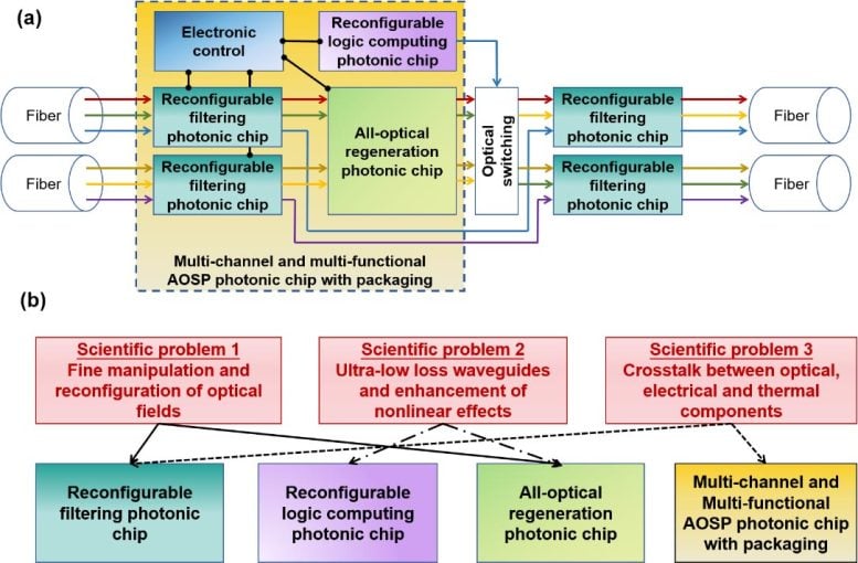
A collaborative team of researchers, including Prof. Xinliang Zhang (Huazhong University of Science and Technology), Prof. Yikai Su (Shanghai Jiao Tong University), Prof. Kun Qiu (University of Electronic Science and Technology of China), and Academician Ninghua Zhu (Nankai University), has successfully developed a monolithically integrated, programmable all-optical signal processing (AOSP) chip. This chip supports key functions such as optical filtering, signal regeneration, and logic operations. The project stems from a national initiative aimed at creating silicon-based, reconfigurable AOSP technologies.
By leveraging the core strengths of silicon photonics—such as CMOS compatibility, minimal signal loss, compact form factor, and strong optical nonlinearities—the researchers have produced a chip capable of meeting the rigorous demands of next-generation optical networks.
These include high-speed data transmission, compatibility with advanced modulation formats, and support for wavelength-transparent operations. The team has experimentally validated the chip’s ability to perform dynamic filtering, logic computation, and signal regeneration, establishing a solid foundation for its use in cutting-edge applications across optical communications, advanced computing, imaging, and sensing.
Overcoming silicon photonics limitations
Developing a programmable all-optical signal processing (AOSP) platform on silicon-on-insulator (SOI) technology presents several technical obstacles. One major issue is that silicon exhibits carrier-related effects—specifically, two-photon absorption (TPA) and free carrier absorption (FCA)—which limit the amount of power that can be used for nonlinear interactions, thereby weakening those effects. Additionally, the high refractive index contrast in silicon leads to tight confinement of the light field, which increases scattering losses, complicates the precise control of light propagation, and introduces significant optical and thermal crosstalk.
To overcome these limitations, researchers have introduced improved fabrication methods, innovative device structures, and novel materials. One of the key advances involves the development of ultra-low-loss silicon waveguides and high-quality microresonators through enhanced manufacturing techniques. These components support integrated photonic filters that offer a broad, reconfigurable bandwidth and tunable free spectral range, allowing for highly flexible and accurate manipulation of input light signals.
In parallel, new design strategies have been implemented to strengthen nonlinear optical performance. These include structures such as ridge waveguides with reverse-biased PIN junctions, slot waveguides, multimode waveguides, and parity-time symmetric coupled microresonators. These configurations enable a range of sophisticated AOSP functionalities. For instance, 100 Gbit/s logic operations have been achieved using a custom-designed single-chip programmable optical logic array. The platform also supports high-dimensional, multi-valued logic processing based on four-wave mixing. Furthermore, highly efficient silicon PIN waveguides have enabled robust multi-channel amplitude and phase regeneration across various signal formats, with demonstrated potential for spatial scaling of regenerative capacity.
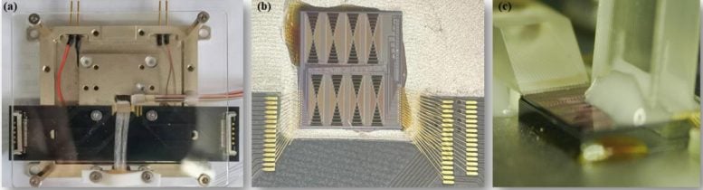
To address the challenges of optical and thermal interference in densely integrated systems, the team developed advanced optical layouts and packaging techniques. These innovations support compact, multi-functional chips with low energy consumption. As a result, four distinct programmable AOSP chips have been realized: a reconfigurable photonic filter chip, a logic processing chip, a multi-dimensional regeneration chip, and a packaged multi-channel, multi-function AOSP chip.
Chip performance metrics and future outlook
This study highlights the key progress in the development of programmable AOSP chips. Through structural and material innovation, key challenges in building large-scale integrated AOSP photonic chips have been addressed, such as high transmission loss, weak nonlinear effects, limited optical field control, and severe optical, electrical, and thermal crosstalk. The loss of ultra-low loss silicon waveguide is as low as 0.17dB/cm, and the Q factor is as high as 2.1106.
We have achieved advanced integrated filters with a bandwidth that can be tuned from 0.55 pm to 648.72 pm (i.e. tuned by more than three orders of magnitude), as well as FSR that can be tuned from 0.06 nm to 1.86 nm (30 times). The absolute FWM conversion efficiency has been proven to be as high as 12 dB, and such high efficiency is crucial for ensuring the success of high-performance logic and regeneration operations.
Eight channel multifunctional single-chip integration of filtering, logic, and regeneration has been achieved, integrating 136 devices (including filters, logic gates, regenerators, gratings, MMIs, electrodes, etc.) on a single chip. It has been proven that the total signal processing capability is up to 800 Gb/s (running at 100 Gb/s per channel), and can accommodate multiple modulation formats, including DPSK and OOK. A complete set of CLU has been generated for logical operations, and QPSK regeneration has been proven to increase receiver sensitivity by more than 6dB. By utilizing advanced optoelectronic packaging technology, the chip level routing and processing of multi-channel signals have been validated.
Due to the inherent ultrafast nature of optical Kerr nonlinearity (on femtosecond timescales), these efforts have laid the foundation for designing and manufacturing larger scale silicon-based AOSP chips at higher speeds. Looking ahead, improvements in nanomanufacturing technology, new materials, and packaging processes are expected to further enhance the performance and flexibility of AOSP chips, highlighting high-efficient and high-density information processing in future classical and non-classical communication and computing applications.
Reference: “Progress in silicon-based reconfigurable and programmable all-optical signal processing chips” by Jing Xu, Wenchan Dong, Qingzhong Huang, Yujia Zhang, Yuchen Yin, Zhenyu Zhao, Desheng Zeng, Xiaoyan Gao, Wentao Gu, Zihao Yang, Hanghang Li, Xinjie Han, Yong Geng, Kunpeng Zhai, Bei Chen, Xin Fu, Lei Lei, Xiaojun Wu, Jianji Dong, Yikai Su, Ming Li, Jianguo Liu, Ninghua Zhu, Xuhan Guo, Heng Zhou, Huashun Wen, Kun Qiu and Xinliang Zhang, 12 May 2025, Frontiers of Optoelectronics.
DOI: 10.1007/s12200-025-00154-6
Funding: National Key Research and Development Program of China
Never miss a breakthrough: Join the SciTechDaily newsletter.